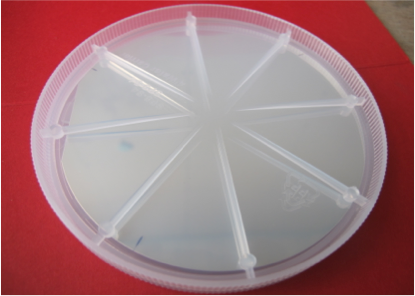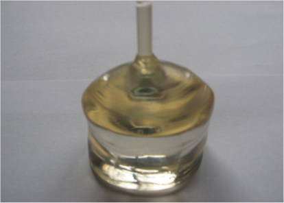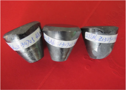
Product Details:
Place of Origin: China
Brand Name: OEM
Certification: ISO9001
Payment & Shipping Terms:
Minimum Order Quantity: Negotiable
Price: Negotiable
Packaging Details: 100g/bag or single wafer box packaging.
Delivery Time: 5-7 working days after receiving payment details
Payment Terms: T/T, Western Union, L/C
| Name: | Nb Doped SrTiO3 | Resistivity: | 0.1 ~ 0.001 Ohm – Cm |
|---|---|---|---|
| Thickness: | 0.5mm Or 1.0mm Or Other Thickness The Customers Request | Surface: | One Side Polished Or Both Sides Polished |
| Doping Concentration: | 0.01 ~ 0.001 Wt % | Mobility (cm2/Vs): | 6.5-9 |
| High Light: | silicon wafer substrate,silicon oxide wafer | ||
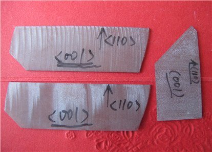
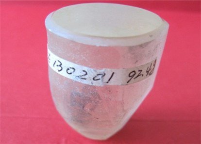
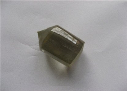
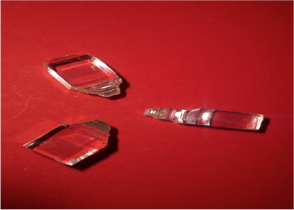
Nb doped SrTiO3 single crystal substrate provide the electrode to the films and devices
Breif intruduction of Nb doped SrTiO3 single crystal substrate
Niobium doped strontium titanate and strontium titanate crystal has the similar structure, but NSTO has electrical conductivity.
Resistivity change range between 0.1 ~ 0.001 ohm – cm, according to the doping concentration between 0.01 ~ 0.001 wt %. Provide the electrode to the films and devices.
Typical Physical Properties of Nb doped SrTiO3 single crystal substrate
Doping concentration and resistivity corresponding table: | ||||||
Nb doped SrTiO3 Grade | A | B | C | D | ||
Nb Concentration (wt%) | 1 | 0.7 | 0.4 | 0.1 | ||
Resistivity (ohm-cm) | 0.0035 | 0.007 | 0.05 | 0.08 | ||
Mobility (cm2/Vs) |
| 9 | 8.5 | 8.5 | 6.5 | |
Standard size of Nb doped SrTiO3 single crystal substrate
5 x 3 mm
5 x 5 mm
6.35×6.35mm
10x5mm
10x10mm
12.7×12.7mm
15x15mm
Thickness of Nb doped SrTiO3 single crystal substrate
0.5mm or 1.0mm or other thickness the customers request
Surface of Nb doped SrTiO3 single crystal substrate
One side polished or both sides polished